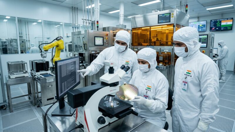
Government Expands National Chip Ambitions with ₹1.27 Lakh Crore Outlay
The Union Cabinet has officially approved the second phase of the India Semiconductor Mission (ISM 2.0), allocating an expanded outlay of ₹1.27 lakh crore ($15 billion) over a 12-year horizon. Building on the foundational investments of Phase 1, ISM 2.0 transitions India’s semiconductor roadmap from basic assembly and testing toward full vertical integration, encompassing commercial silicon fabrication, advanced 3D packaging, specialized equipment manufacturing, and high-purity chemical supply chains.
Under the revised scheme, the government will provide financial subsidies ranging from 25% to 40% for eligible semiconductor fabrication plants (fabs), compound semiconductor facilities, and OSAT (Outsourced Semiconductor Assembly and Test) hubs. The extended 12-year program lifecycle is specifically designed to provide long-term regulatory and fiscal certainty for global chipmakers considering major multi-stage capital commitments in India.
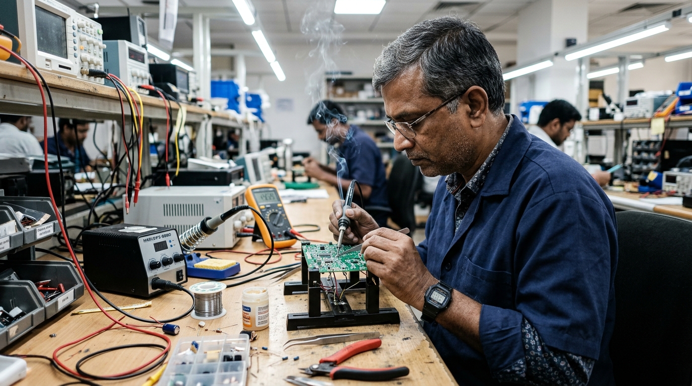
Navigating Global Capex Realities Against Semiconductor Giants
While India’s ₹1.27 lakh crore incentive package represents a landmark domestic commitment, industry experts emphasize the massive scale gap compared to global foundry titans. For context, Taiwan Semiconductor Manufacturing Company (TSMC) alone deploys over $30 billion to $35 billion in annual capital expenditure. Consequently, India’s strategy focuses on specialized trailing-edge nodes (28nm to 65nm), power electronics, and automotive microcontrollers rather than competing immediately in sub-2nm leading-edge processes.
This targeted approach aligns perfectly with India’s expanding domestic electronics manufacturing ecosystem, which consumes vast quantities of mature-node chips for automotive, industrial automation, telecom gear, and consumer appliances. Facilities like Tata Electronics’ Dholera fab and CG Power’s Sanand OSAT unit are slated to anchor this domestic supply chain, reducing reliance on East Asian chip imports.
Building R&D Talent and Specialized Supply Chain Infrastructure
Beyond physical fab construction, ISM 2.0 reserves substantial funding for electronic design automation (EDA) software licenses and semiconductor R&D hubs across premier Indian institutes. By nurturing a nation-wide pool of chip design engineers, India aims to build high-margin intellectual property (IP) locally, laying the foundation for a sustainable, self-sufficient semiconductor ecosystem over the next decade.
Disclaimer: This article is for informational purposes only and does not constitute investment advice, a recommendation, or a solicitation to buy or sell any securities. The views expressed are those of the author and do not represent the official position of Benzinga India. Readers should consult a SEBI-registered financial advisor before making any investment decisions. Benzinga India and its authors do not hold any positions in the securities mentioned in this article unless explicitly stated.